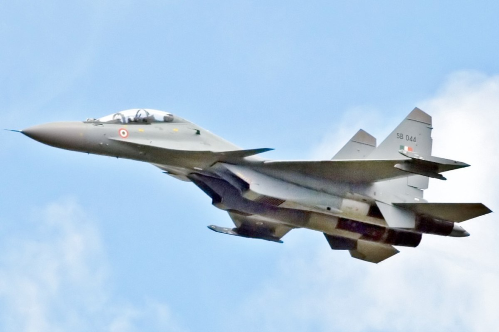
DRDO’s Electronics and Radar Development Establishment (LRDE) is starting fabrication of the Virupaksha radar for the Indian Air Force’s Su-30MKI upgrade. They are setting up two assembly jigs to begin ground testing soon.

Tight Assembly and Testing Timeline
LRDE plans to deliver two fully assembled jigs within 16 weeks of the contract’s approval. The team aims to finish the assembly in 15 weeks. They will use the final week for acceptance testing. This efficient timeline highlights their commitment to delivering on time and maintaining high standards.

Advanced Radar Architecture
The Virupaksha radar brings major improvements over earlier designs, like the Uttam radar. Unlike Uttam’s quad TRM-based system, the Virupaksha radar uses eben more densely packed design. It incorporates planks, which make maintenance and testing easier. The tighter packing results in more compact components without compromising functionality.
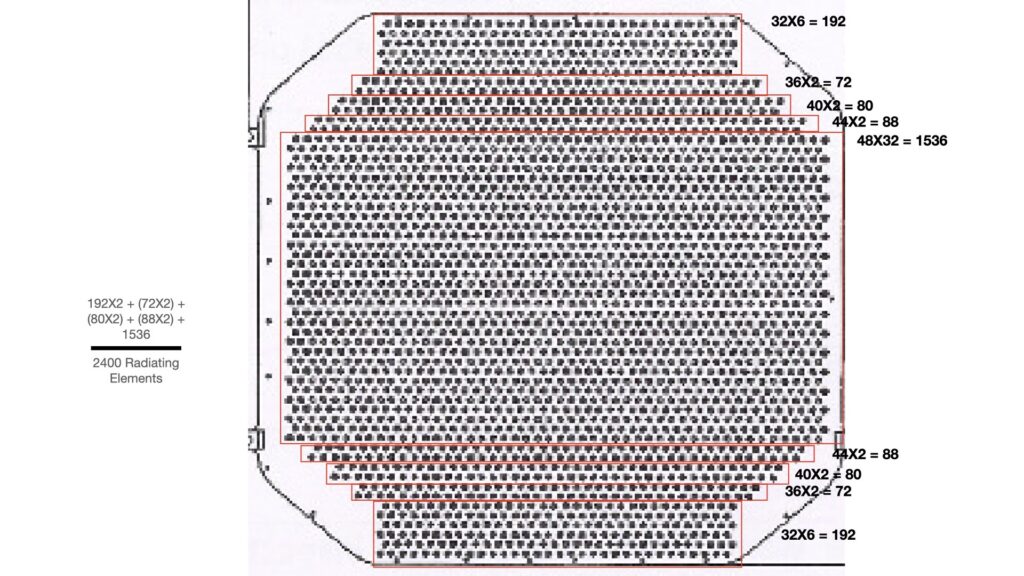
The schematic of this radar suggests it will be a monstrous radar with nearly 2400 radiating elements closely packed in GaN based planks.

This design uses Gallium Nitride (GaN) technology, which improves power efficiency and thermal performance. GaN allows higher power density, creating a smaller yet more efficient radar system. This enables the radar to deliver superior performance while simplifying maintenance.
Why Nitride is Important ?
The impact of GaN (Gallium Nitride) technology on radar range, particularly in AESA (Active Electronically Scanned Array) applications, is significant when compared to GaAs (Gallium Arsenide) due to GaN’s higher efficiency, power density, and thermal management capabilities.
- Power Output: GaN transistors can achieve output powers of up to 200 W per element in AESA radars, significantly boosting radar range. For long-range systems, GaN’s ability to operate at higher power levels means the radar can detect objects farther away. GaAs-based systems typically deliver lower power outputs, thus limiting the radar’s range in comparison.
- GaAs: Typically, GaAs transistors offer a power density of about 1.5 W/mm, with power outputs ranging from 5-10 watts, though higher outputs up to 40 watts can be achieved using multiple devices in parallel or push-pull configurations. However, this comes at the cost of reduced efficiency and increased space for peripheral circuitry
- GaN: In contrast, GaN can deliver power densities up to 5 times higher than GaAs, with outputs ranging from tens to hundreds of watts per transistor. For instance, GaN transistors on silicon carbide (GaN-on-SiC) substrates can reach output levels of up to 200 W in AESA systems.
- Thermal Efficiency: GaN offers about 15% better thermal conductivity than GaAs, allowing radar systems to operate at higher temperatures and power densities without overheating. This efficiency translates into fewer cooling requirements and allows radars to sustain longer operational periods at maximum performance, which in turn improves the radar’s continuous detection range.
- GaAs: GaAs has a lower thermal conductivity, typically around 46 W/mK. This limits its ability to dissipate heat effectively, which restricts high-power operation in radar systems. GaAs transistors tend to overheat at higher power levels, reducing overall system efficiency and requiring complex cooling solutions.
- GaN: GaN has a thermal conductivity of around 130-170 W/mK, which is more than 3 times higher than GaAs. This allows GaN devices to operate at much higher power densities while maintaining efficient heat dissipation. The increased thermal conductivity means GaN-based systems can handle higher temperatures without performance degradation, leading to more compact and efficient AESA radar designs.
- Bandwidth: GaN-based radars also operate at higher frequencies than GaAs systems. This enables greater bandwidth for signal transmission, resulting in better resolution and sensitivity at long ranges. This advantage is crucial in AESA systems where the ability to detect smaller or more distant targets is a priority.
- GaAs : GaAs can handle moderate bandwidths, but its performance tends to degrade in multi-frequency or high-power applications at the upper end of the X-band.
- GaN : GaN transistors allow for wider bandwidths, crucial for multi-function radars that need to operate across multiple channels simultaneously. GaN can support higher instantaneous bandwidths (tens of GHz) within the X-band, enabling AESA radars to cover a larger frequency spectrum and process more data in real-time. This makes GaN based AESA immune to GaAs based Radar jammers.
- System Longevity: GaN’s inherent material properties lead to longer operational lifespans, which reduces maintenance costs and increases reliability in high-demand, long-range detection systems. This improves overall system uptime and range capability over the radar’s lifecycle.
These factors together mean that when using GaN in AESA radars, the range can be extended by up to 50% compared to GaAs by very conservative estimate, depending on the specific radar application and power constraints.
Strengthening India’s Air Superiority
With testing starting soon, the Virupaksha radar will significantly enhance the Su-30MKI’s capabilities. It offers better tracking, targeting, and situational awareness, supporting India’s defense modernization. LRDE’s work ensures the Indian Air Force continues to strengthen its air superiority with state-of-the-art radar systems.

Wonderful article
The entire Su-30 fleet should get this Virupaksha radar. With the delay in the, arrival of new fighters in large numbers, the Su-30s are the lifeline of IAF for at least the next 20 years.
very nice article, scientifically explained. the author know some thing
kepp it up, many more from him pse
wht is this article so technically detailed ? isnt it laying bare the design of radar for which ever adversary to see…
whats the point in being so detailed about technical internals of the radar in public domain…